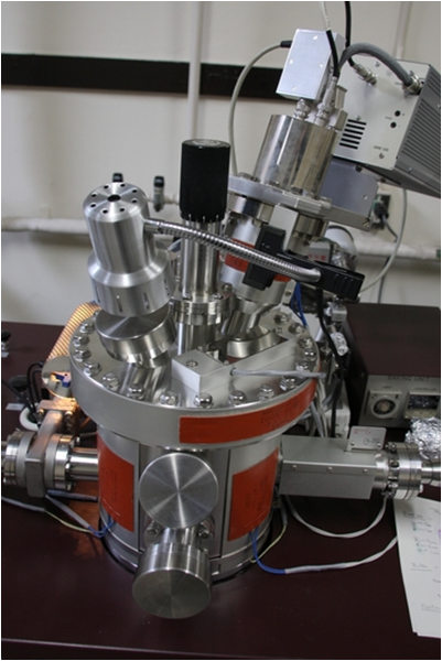
| RESEARCH ACTIVITIES | ||
Main topics are listed below and related issues are also in progress. (1) High-k Dielectrics (2) Germanium Renaissance (3) 2D semiconductor properties (4) Functional oxide (VO2, TiO2) FET |
||
| (1) High-k Dielectrics | ||
| Multi-component High-k Film Deposition | ||
 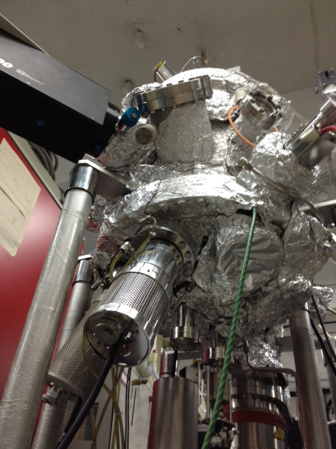
|
||
|
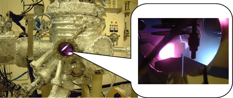
Multi-target magnetron sputtering
|
Molecular Beam Epitaxy (MBE)
|
|
Pulse Laser deposition |
Laser ablation of targets | |
Various properties of oxides can be designed by controlling the microscopic structures. |
||
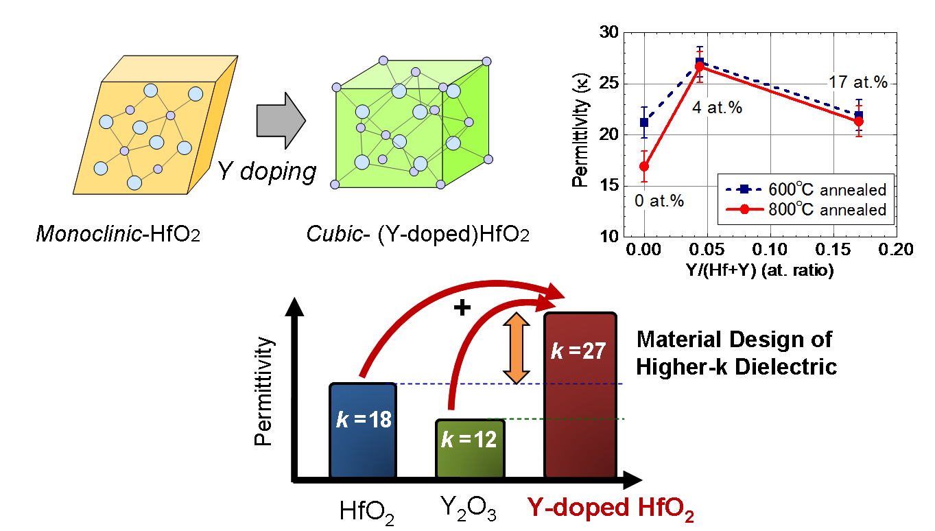
| Permittivity Enhancement by Structural Control | ||
 |
||
In SSDM 2004 (K. Kita et al.) we have demonstrated, a dramatic enhancement of dielectric constant of HfO2 approaching ~30 by a crystal-structure modification of HfO2 for the first time in the world. This is realized by doping of different oxides, such as Y2O3, into HfO2 [K. Kita et al., APL 2005.]. This concept enables us to design several types of novel higher-k ternary oxides including Si-doped HfO2[K. Tomida et al., APL 2006], LaYOx [Y. Zhao et al., APL 2009], and LaTaOx [Y. Zhao et al., JAP 2009]. |
||
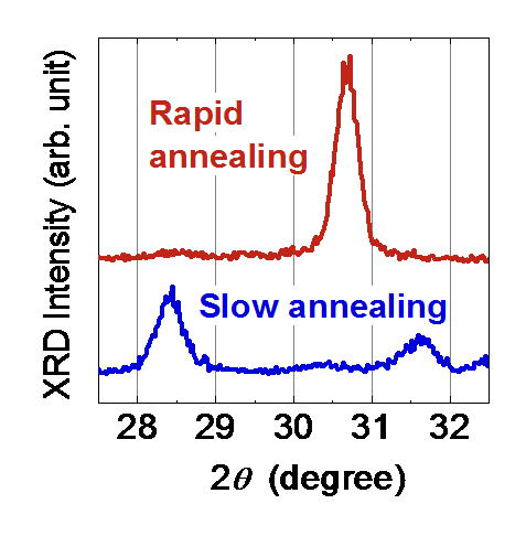
| Structural Control of High-k Dielectrics by Rapid Thermal Treatment | ||
 |
||
Rapid thermal annealing |
||
We have started to investigate the structural control of High-k films without doping, but with an ultrafast thermal processes. Since HfO2 has a tendency to start to crystallize in a higher-symmetric structure followed by a transformation to the monoclinic structure [Y. Nakajima et al., ECS Trans. 2010], the dielectric properties of HfO2 is largely controllable by tuning the time and temperature. Now we are extending the phase control to Ferro-HfO2. |
||
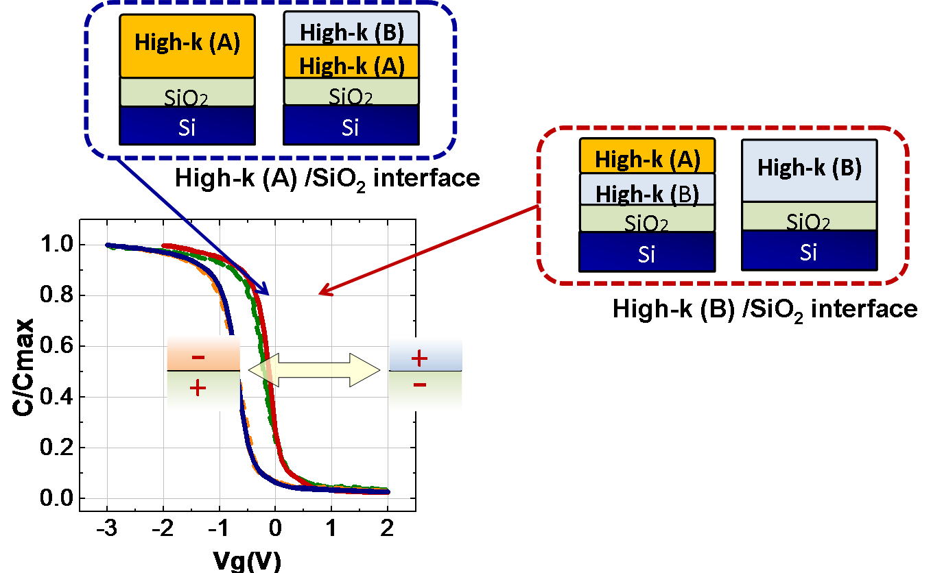
| Dipole Layer Formation between Two Oxides | ||
Tuning the threshold voltage is one of the critical issues in high-k/metal gate (HK/MG) technologies. It is because the flatband voltage (VFB) of HK/MG stack shows a significant shift depending on the employed high-k materials. In 2006 (Y. Yamamoto et al., SSDM 2006, Yokohama), we have clarified that the one of the most important factor to determine the unexpected VFB shift is due to the dipole layer formation at high-k/SiO2 interface [Y. Yamamoto et al., JJAP 2007]. |
||
 |
||
 |
||
 |
||
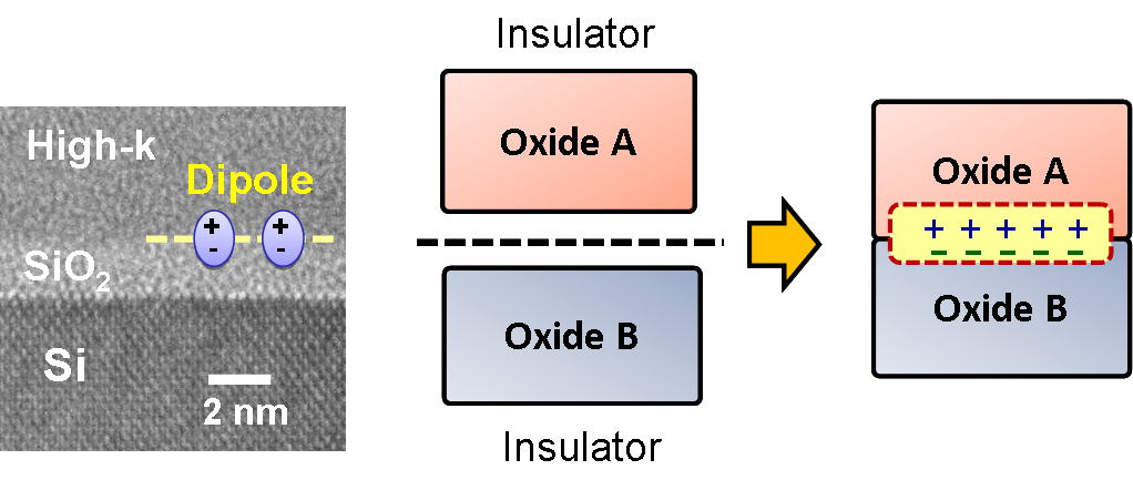
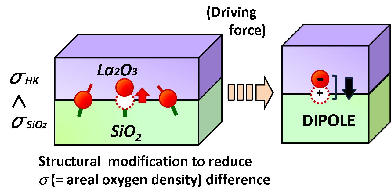
In 2008 (K. Kita and A. Toriumi, IEDM 2008, San Francisco) we have also proposed a possible physical origin of the dipole formation at high-k/SiO2 interface. The structural difference between two oxides will be the key factor to determine the direction / strength of the driving force to form a dipole [K. Kita and A. Toriumi, APL 2009] |
||
| (2) Germanium Renaissance | ||
| GeO desorption caused by GeO2/Ge interfacing | ||
|
||
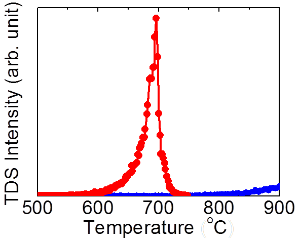
| Thermal desorption spectra of GeO and its instrument. | Ge (111) substrate surface in oxygen at 700oC | |
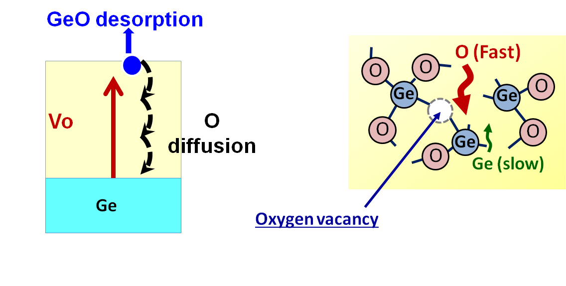
Thermally unstable GeO2 electrically degrade channel interface of Ge MOSFET with GeO desorption. At first, we focused on substrate dependence of GeO desorption. The figure shows temperature desorption spectrometer (TDS) signal of GeO[K. Kita et al., JJAP 2008]. Low temperature GeO desorption is caused by direct GeO2/Ge interfacing, and it is caused by the reaction of Ge + GeO2 -> 2GeO. |
||
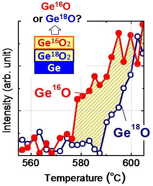
| Mechanism of GeO desorption - Diffusion species - | ||
 |
||
GeO desorption is limited by diffusion process in GeO2[S. K. Wang et al., JAP 2010]. Now, we are focusing on the diffusing species by isotope marker. The figure is the GeO signal measured by thermal desorption spectrometer (TDS). Oxygen of desorbed GeO derives from top-side GeO2 and that GeO itself is not diffusion species[K. Kita et al., IEDM 2009]. |
||
| GeO2 bulk degradation by GeO desorption | ||
 |
||
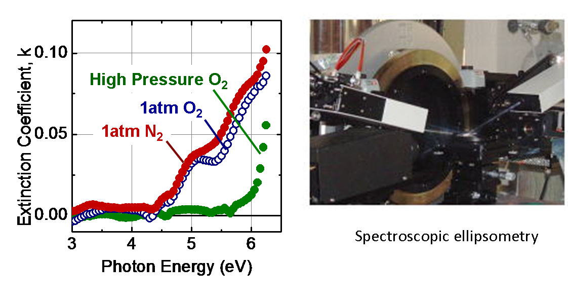
Extinction coefficients of various GeO2 estimated by spectroscopic ellipsometry. To obtain electrically excellent GeO2/Ge interface, high pressure oxidation which thermodynamically and kinetically suppresses GeO desorption from GeO2/Ge stack [C. H. Lee et al., APEX 2009]. Additionally, high pressure oxygen annealing affects bulk GeO2 film quality. Sub-gap absorption (<6 eV) level is expected to be formed by GeO desorption [K. Kita et a l., IEDM 2009]. |
||
| High pressure oxidized GeO2/Ge interface | ||
 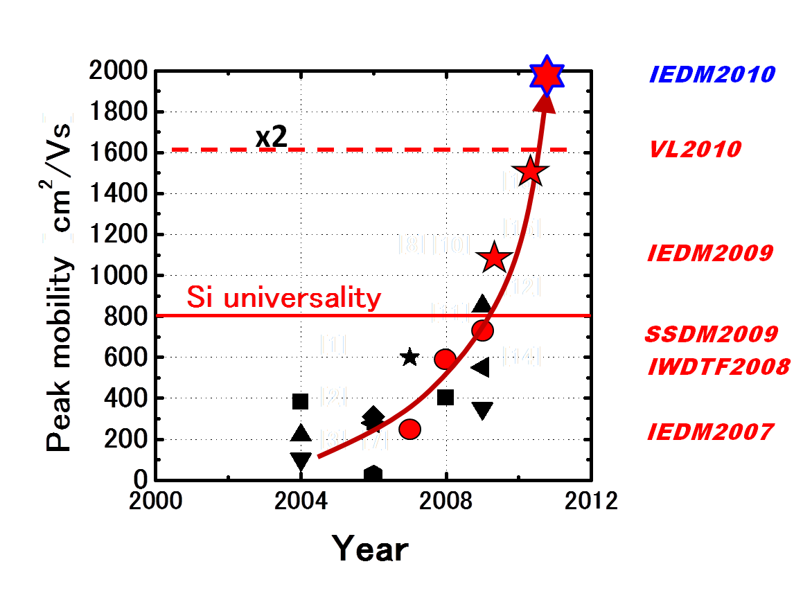 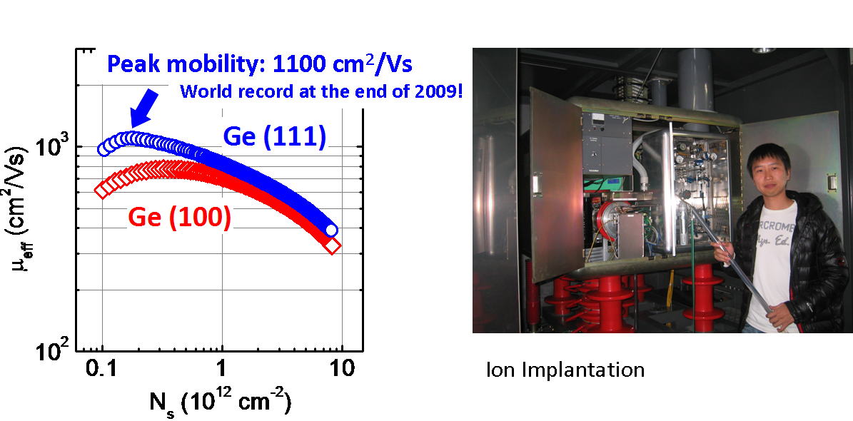 Electron inversion layer mobility of Ge (100) and (111) nMOSFET with GeO2 gate stacks formed by high pressure oxidation [C. H. Lee APEX 2009]. Ge (111) should be better in terms of the lower effective mass in two dimensional inversion layer* and higher process stability [M. Toyama et al., SSDM 2004] . The peak mobility on Ge (111) is about 1100cm2/Vs at 300K and it is 1.5 times improved compared to that of Si Universal curve. |
||
| Ge friendly high-k material & High pressure oxidation | ||
 |
||
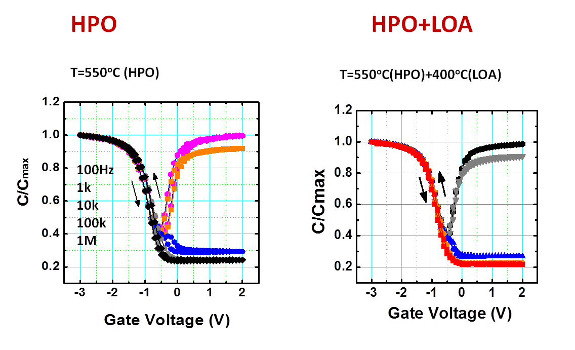
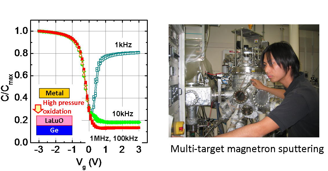
C-V characteristics of LaLuO(rare-earth oxide)/Ge MIS capacitor with high pressure oxidation. High-k gate dielectric is required for enhancement of Ge MOSFET performance by scaling. We reported advantage of rare-earth oxides on Ge from the viewpoint of interfacial electrical characteristics [K. Kita et al., Appl. Surf. Sci. 2008]. Furthermore, combining this Ge friendly rare-earth oxide with high pressure oxidation (through rare-earth oxide), almost ideal C-V characteristics are obtained [T. Tabata et al., ECS Trans. 2008]. Now we are focusing on a role of rare-earth atom in interfacial passivation. |
||
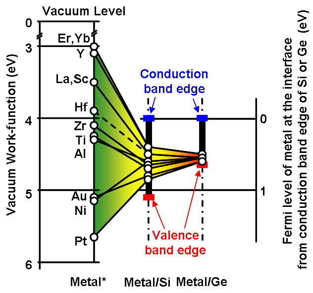
| Strong Fermi level pinning at metal/Ge interface | ||
 |
||
At metal/Ge contact, band alignment is hardly determined by work function of metal. Fermi level of metal is strongly pinned to the valence band edge of Ge, hence Schottky characteristics is observed on n-type Ge and ohmic ones on p-type Ge irrespective to metal [T. Nishimura et al., APL 2007]. The origin of this strong pinning has not been clarified. |
||
| Tunnel contact | ||
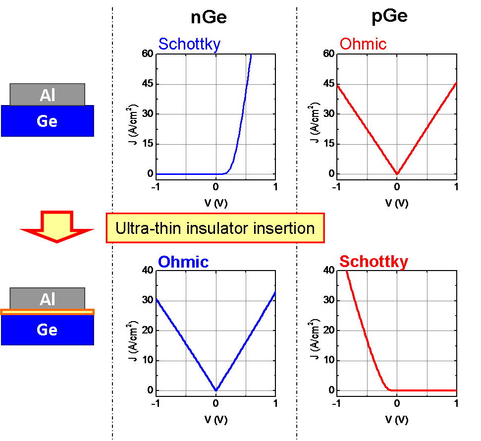 Complete junction characteristics conversion (Schottky-ohmic conversion) by ultra-thin insulator insertion at metal/Ge interface. We found out that the strong Fermi level pinning at metal/Ge interface can be easily modulated only by ultra-thin insulator insertion[T. Nishimura et al., APEX 2008]. This is a key to understanding a guiding principle of band alignment formation at hetero junction. |
||
| (3) 2D semiconductor properties |
||
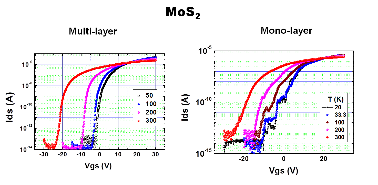
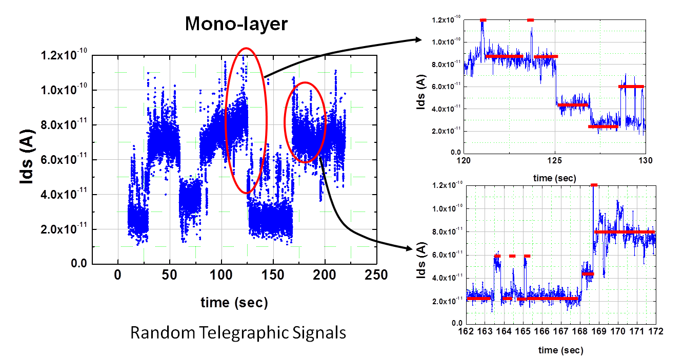
Graphene research has moved to Nagashio’s Lab. since April, 2014. Then, we have just launched TMD(transition metal dichalcogenide) research. Now, MoS2 is under investigation. The result seems to be quite interesting. |
||
 |
||
 |
||
| (4) Functional Oxide FET A range of functionalities in transition metal oxides, which are absent in conventional semiconductors, are controlled on the common device platform of Thin Film Transistor (TFT), aiming at interdisciplinary functional electronic devices. |
||
| Metal-Insulator Transition in VO2 | ||
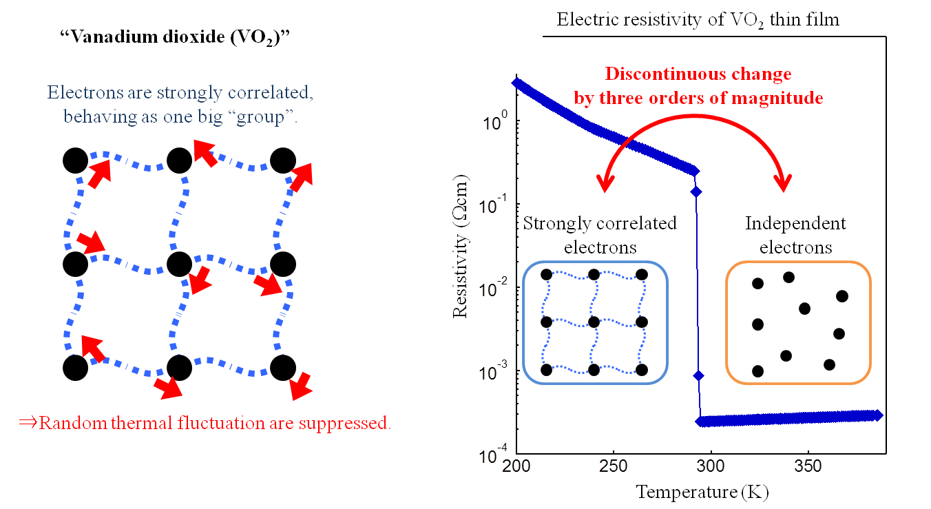 Electrons in VO2 behave as a group, suppressing fluctuation of each individual electron (left). As a result, VO2 shows a sharp phase transition between metallic phase and insulating phase (right). |
||
| Domain structures of metallic/insulating phases during metal-insulator transition | ||
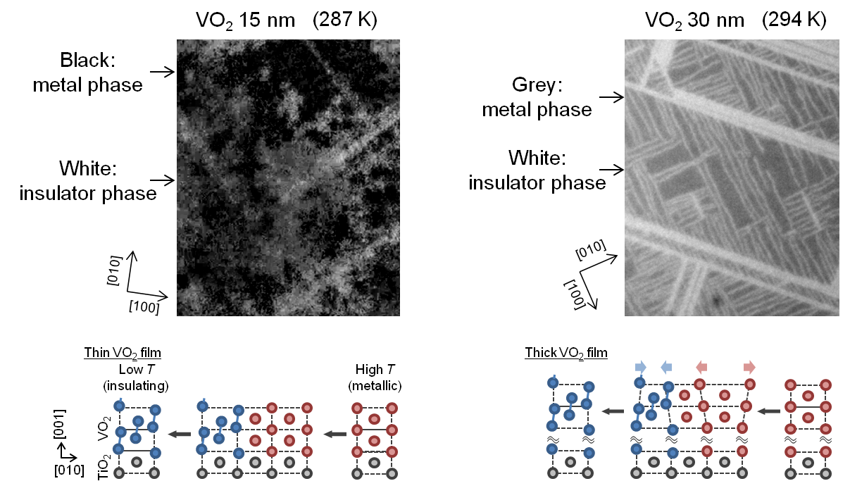 When the VO2 film is thin, strech/contraction of VO2 unit cells is suppressed, leading to the random distribution of metallic/insulating phases (left). As the VO2 film becomes thick, strech/contraction of VO2 unit cells is allowed, forming the well-ordered pattern of metallic/insulating phases (right). |
||
| Interaction between two neighboring phase transitions | ||
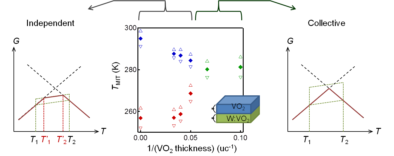 VO2 and W-doped VO2 show two independent metal-insulator transitions. However, in a very thin regime, the two transitions interact and mearge into a single intermediate transition. (middle). Physics behind it is that when the domain boundary energy exceeds the free energy of each thin layer, the independent transitions are no longer energetically stable. (left and right). |
||
| TiO2-channel thin film transistor | ||
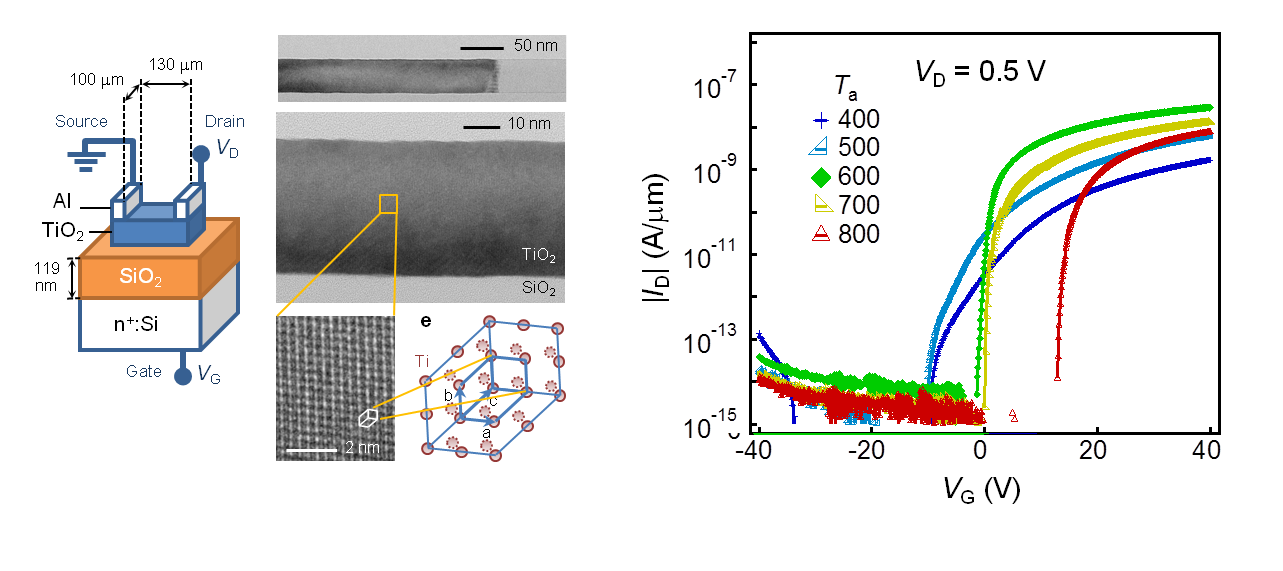 TiO2-channel thin film transistor can be fabricated on Si substrate. (left). By fine-tuning the thermal treatment conditions, the field effect mobility reaches 10 cm2/Vs, comparable to IGZO-channel (right). |
||
Inquiries on this page to ⇒ nishimura at material.t.u-tokyo.ac.jp (at->@)