Tunnel FET is expected to be low power FET because small SS is able to be achieved. However, in general, it suffers from the low on current, due to the tunneling nature. By applying 2D layered materials to TFET, high on current may be possible because of short tunneling distance (van der Waals distance). We are studing 2D-TFET. [collaborated with Prof. Ueno@Saitama univ. & Dr. Taniguchi, Watanabe@NIMS]
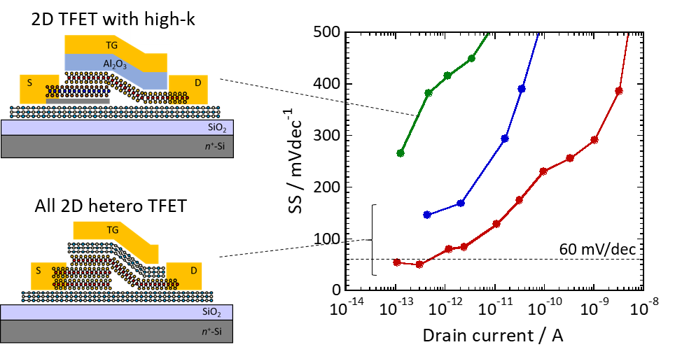
##(Left) 2D TFET with high-k and all 2D hetero TFET were fabricated. SS < 60 mV/dec was achieved in all 2D hetero TFET. (Nakamura, 2020,3).
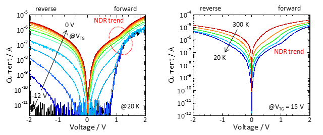
##(Left) In diode characteristics, it is clear that the band alignment changes from type II to type III by applying the gate voltage. (Right) NDR trend is observed with decreasing the temperature. This indicates that the reverse bias current is band to band tunneling current.(Nakamura, 2020.3 & He, 2018.3)
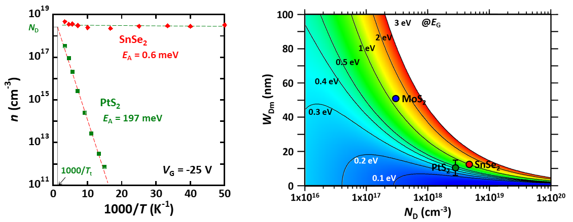
##(Left) For candidates of N+-crystals, carrier densities of SnSe2 and PtS2 were determined by Hall measurments. SnSe2: 4.7*1018 cm-3, PtS2: 3.6*1017 cm-3. SnSe2 is proper for N+ source.(Sato, 2021.3)
Ref.
Hiroto Ogura, Seiya Kawasaki, Zheng Liu, Takahiko Endo, Mina Maruyama,Yanlin Gao, Yusuke Nakanishi, Hong En Lim, Kazuhiro Yanagi, Toshifumi Irisawa, Keiji Ueno, Susumu Okada, Kosuke Nagashio, Yasumitsu Miyata, “Multilayer In-Plane Heterostructures Based on Transition Metal Dichalcogenides for Advanced Electronics”, ACS nano, 2023, 17, 7, 6545-6554.
Y. Sato, T.Nishimura, D. Duanfei, K.Ueno, K. Shinokita, K. Matsuda and K. Nagashio, "Intrinsic Electronic Transport Properties and Carrier Densities in PtS2 and SnSe2: Exploration of n+-Source for 2D Tunnel FET", Adv. Electronic Mater., 2021, (in press).
K. Nakamura, N. Nagamura, K. Ueno, T. Taniguchi, K. Watanabe, K. Nagashio, “All 2D heterostructure Tunnel Field Effect Transistors: Impact of Band Alignment and Heterointerface Quality”, ACS Applied Materials & Interfaces, 2020, 12, 51598−51606.
J. He, N. Fang, K. Nakamura, K. Ueno, T. Taniguchi, K. Watanabe, and K. Nagashio, "2-Dimensional Tunnel FETs with a Stable Charge-Transfer-Type p+-WSe₂ Source", Adv. Electronic Mater. 2018, 4, 1800207.
3. Growth, transport & interface properties of MoS2
We are interested in 2D semiconductor with band gap, MoS2. Compared with Kish graphite with high crystallinity, bulk MoS2 includes lots of S vacancies. We have studied how S vacancy affect transport properties of MoS2.
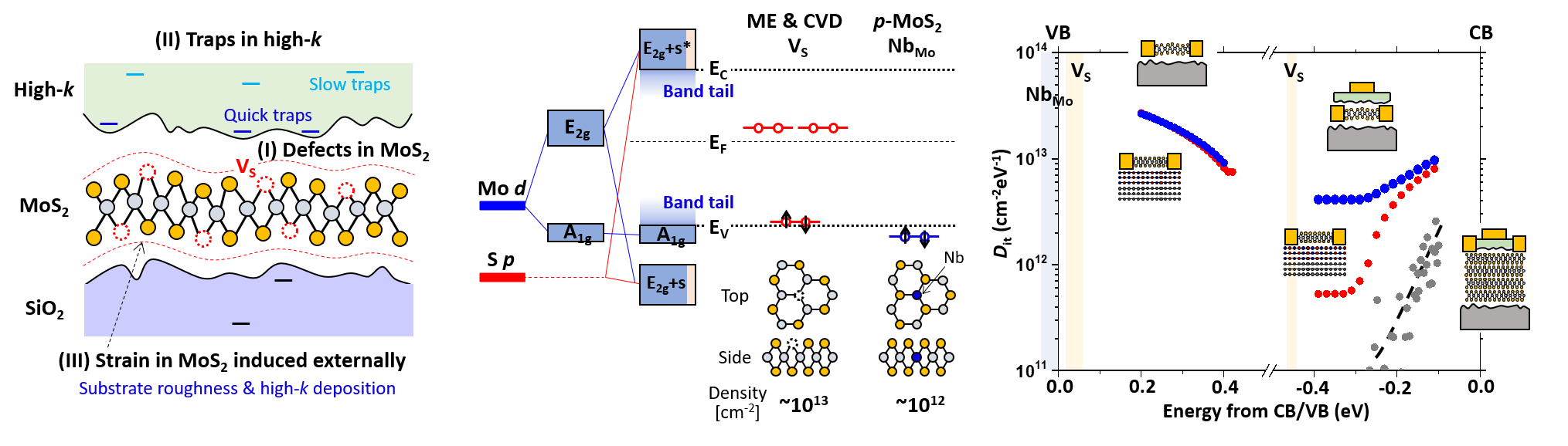
##(Left) Three different origins for Dit in high-k/MoS2/Sio2 gate stack. (Middle) Band strcutre of MoS2 is formed by ligand field. Conduction and valence bands resutls from d-d splitting. S vacancy levels are found at midgap and near the valence band. (Right) Dit as a function of energy. DIt can be reduced by reducing the strain in MoS2 by heterostructure formation. (Nan Fang & Toyoda, 2019)
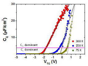
##Quantum capacitance as a function of top gate voltage for monolayer MoS2.(2018, Nan Fang) JSAP Young Researcher award
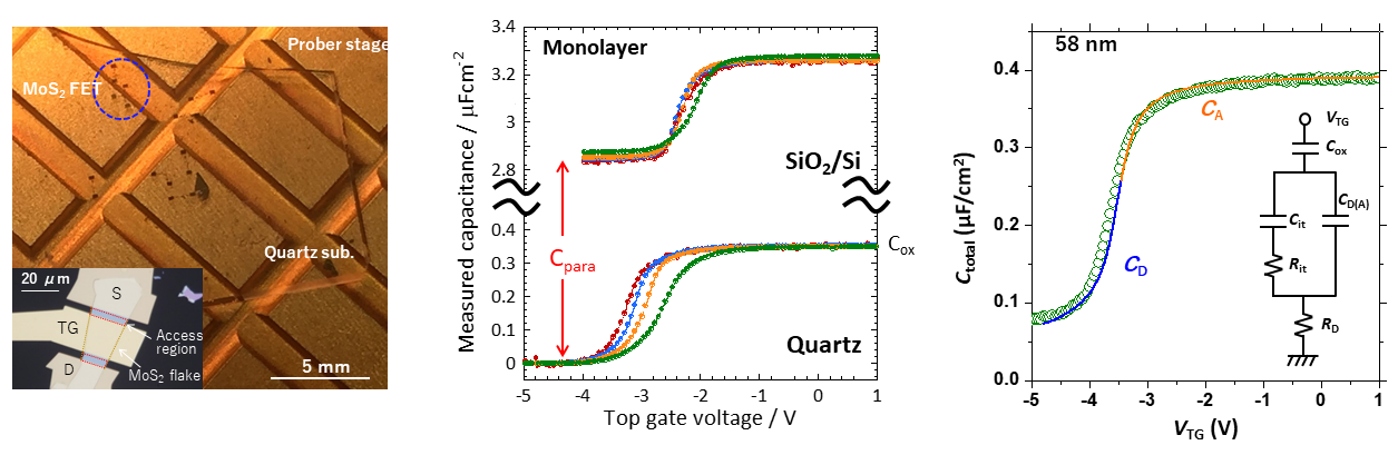
##(Left) Monolayer MoS2 top gate FET on quartz substrate. (Middle) Measured capacitance vs VTG for MoS2 FET on SiO2/Si and quartz substrates. (Right) Capacitance vs VTG for thick MoS2 FET on quartz. Depletion capacitance can be clearly determined due to no parasitic capacitance (on quartz). (2018, Nan Fang)
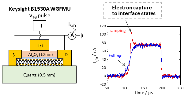
##(Left) Time domain charge pumping experiment was applied to MoS2 FET. (Right) Electron capture and emission behavior was clearly observed. (2018, Taniguchi)
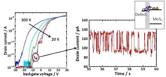
##(Left) Transport properties of MoS2. With decreasing temperature, zigzag feature apppeared. (Right) When gate bias is fixed at the zigzag region, Id was measured as a function of time, showing the random telegraphic noise(RTN). The analysis using the multiterminal device indicates that the trap sites exist within the channel.(2016, Nan Fang) SSDM Young Researcher award
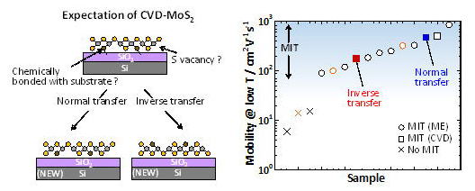
##(Left) For CVD-MoS2, we have investigated which surface includes more S vancacies, top or bottom surface. Two kinds of samples were prepared by normal transfer and inverse transfer. (Right) Both cases showed high mobilities, suggesting the difference in the crystallinity for top and bottom surfaces is negligible. (Kurabayashi, 2017)
Ref.
S. Kurabayashi, and K. Nagashio, ”Transport properties of the top and bottom surfaces in monolayer MoS2 grown by chemical vapor deposition”, Nanoscale, 2017, 9, 13264-13271.
N. Fang, K. Nagashio, and A. Toriumi, “Subthreshold transport in mono- and multilayered MoS2 FETs”, Appl. Phys. Express, 2015, 8, 065203.
N. Fang, K. Nagashio, and A. Toriumi, “Experimental detection of active defects in few layers MoS2 through random telegraphic signals analysis observed in its FET characteristics”, 2D mater., 2017, 4, 015035.
N. Fang, K. Nagashio, “Band tail interface states and quantum capacitance in a monolayer molybdenum disulfide field-effect-transistor”, J. Phys. D, 2018, 51, 065110.
N. Fang, and K. Nagashio, “Accumulation-mode two-dimensional field-effect transistor: Operation mechanism and thickness scaling rule”, ACS appl. mater. interfaces, 2018, 10, 32355.
K. Taniguchi, N. Fang, and K. Nagashio, “Direct observation of electron capture & emission processes by the time domain charge pumping measurement of MoS2 FET”, Appl. Phys. Lett. 2018, 113, 133505.
W. Li, et al., “Uniform and ultrathin high-κ gate dielectrics for two-dimensional electronic devices”, Nature Electronics, 2019, 2, 563–571.
N. Fang, S. Toyoda, T. Taniguchi, K. Watanabe, and K. Nagashio, “Full energy spectra of interface state densities for n– and p-type MoS2 field-effect transistors”, Adv. Func. Mater. 2019, 29, 1904465.
N. Fang and K. Nagashio, “Quantum-mechanical effect in atomically thin MoS2 FET”, 2D mater, 2020, 7, 014001.
Haruki Uchiyama, Kohei Maruyama, Edward Chen, Tomonori Nishimura, Kosuke Nagashio, “A Monolayer MoS2 FET with an EOT of 1.1 nm Achieved by the Direct Formation of a High-κ Er2O3 Insulator Through Thermal Evaporation”, Small, 2023, 19, 2207394.
Shuhong Li, Tomonori Nishimura, Mina Maruyama, Susumu Okada and Kosuke Nagashio, “Experimental verification of SO2 and S desorption contributing to defect formation in MoS2 by thermal desorption spectroscopy”, Nanoscale Adv., 2023, 5, 405-411.
Ryoichi Kato, Haruki Uchiyama, Tomonori Nishimura, Keiji Ueno, Takashi Taniguchi, Kenji Watanabe, Edward Chen, Kosuke Nagashio, “p-type conversion of WS2 and WSe2 by position-selective oxidation doping and its application in top gate transistors”, ACS appl. mater. interfaces, 2023, 15(22), 26977-26984.
4. Piezoelectric/ferroelectric properties of SnS
In 2D materials, monolayer SnS posesses piezoelectric constant similar to that of PZT. We are interested in the energy harvesting using SnS. However, it is difficult to obtain monolayer since interlayer force is composed of ionic contribution as well as vdW. We are trying to obtain monolayer and measuring the electronic/piezoelectric properties. [collaborated with Dr. Nakamura@NIMS, Prof. Ueno@Saitama Univ. & Prof. Wakabayashi, KGU]
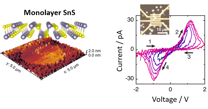
##(Top) By mechanical exfoliation of SnS, the thickness can be reduced, but not to monolayer. The electron transport properties show the p-type conduction due to Sn vacancy. (Bottom) By annealing in O2, monolayer thick SnS was prepared as shown in TEM image. The ambipolar behavior was observed. (2018 Higashitarumizu)
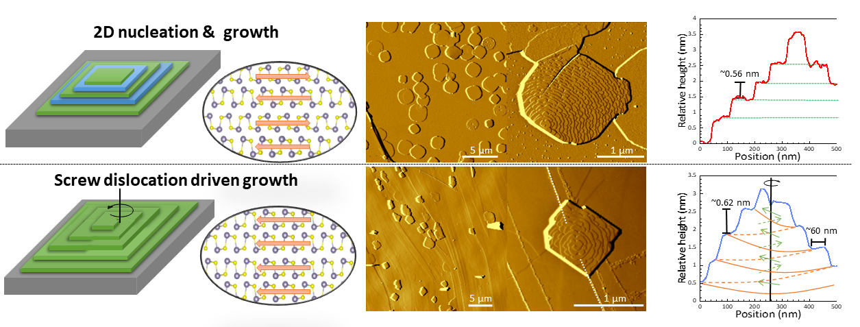
##SnS shows even-odd effect, in which polarization in the layer is cancelled for even layers. In order to enhance the polarization, we need to achieve the same direction of polarization for all layers. Using the graphene steps in HOPG, spiral growth can be possible, which may lead to AA stacking. (2020 Chang)
Ref.
N. Higashitarumizu, H. Kawamoto, K. Ueno and K. Nagashio, “Fabrication and Surface Engineering of Two-Dimensional SnS Toward Piezoelectric Nanogenerator Application”, MRS Advances, 2018, 3, 2809.
N. Higashitarumizu, H. Kawamoto, M. Nakamura, K. Shimamura, N. Ohashi, K. Ueno, and K. Nagashio, “Self-passivated ultra-thin SnS layers via mechanical exfoliation and post-oxidation”, Nanoscale, 2018, 10, 22474.
H. Kawamoto, N. Higashitarumizu, N. Nagamura, M. Nakamura, K. Shimamura, N. Ohashi, and K. Nagashio, “Micrometer-scale monolayer SnS growth by physicalvapor deposition”, Nanoscale, 2020, 12, 23274.
N. Higashitarumizu, H. Kawamoto, C.-J. Lee, B. -H. Lin, F. -H. Chu, I. Yonemori, T.i Nishimura, K. Wakabayashi, W. -H. Chang & K. Nagashio, “Purely in-plane ferroelectricity in monolayer SnS at room temperature”, Nature commun.,2020, 11, 2428.
Yih-Ren Chang, Naoki Higashitarumizu, Hayami Kawamoto, Fu-Hsien Chu, Chien-Ju Lee, Tomonori Nishimura, Rong Xiang, Wen-Hao Chang, Shigeo Maruyama, Kosuke Nagashio, “Atomic-Step-Induced Screw-Dislocation-Driven Spiral Growth of SnS”, Chem. Mater. 2021, 33, 1, 186–194.
Yih-Ren Chang, Tomonori Nishimura, Takashi Taniguchi, Kenji Watanabe,Kosuke Nagashio, “Performance enhancement of SnS/h-BN Heterostructure p-type FET via Thermodynamically Predicted Surface Oxide Conversion Method”, ACS Appl. Mater. Interfaces., 2022, 14, 17, 19928–19937.
Yih-Ren Chang, Ryo Nanae, Satsuki Kitamura, Tomonori Nishimura, Haonan Wang, Yubei Xiang, Keisuke Shinokita, Kazunari Matsuda, Takashi Taniguchi, Kenji Watanabe, and Kosuke Nagashio, “Shift current photovoltaics based on a noncentrosymmetric phase in in-plane ferroelectric SnS”, Adv. Mater., 2023, 35, 2301172.
. Redhwan Moqbel, Yih-Ren Chang, Zi-Yi Li, Sheng-Hsun Kung, Hao-Yu Cheng, Chi-Cheng Lee, Kosuke Nagashio, Kung-Hsuan Lin, “Wavelength Dependence of Polarization-resolved Second Harmonic Generation from Ferroelectric SnS Few Layers”, 2D mater. 2023, 10, 015022.
4. Underdstanding of operation mechanism of 2D flash memory
High electrial reliability in 2D flash memery has been expected due to dangling bond free 2Dhetero-interface. However, the understanding of operation mechanism in 2D flush memory is quite limitted. We are studying 2D flush memory by constructing 2D heterostacks.
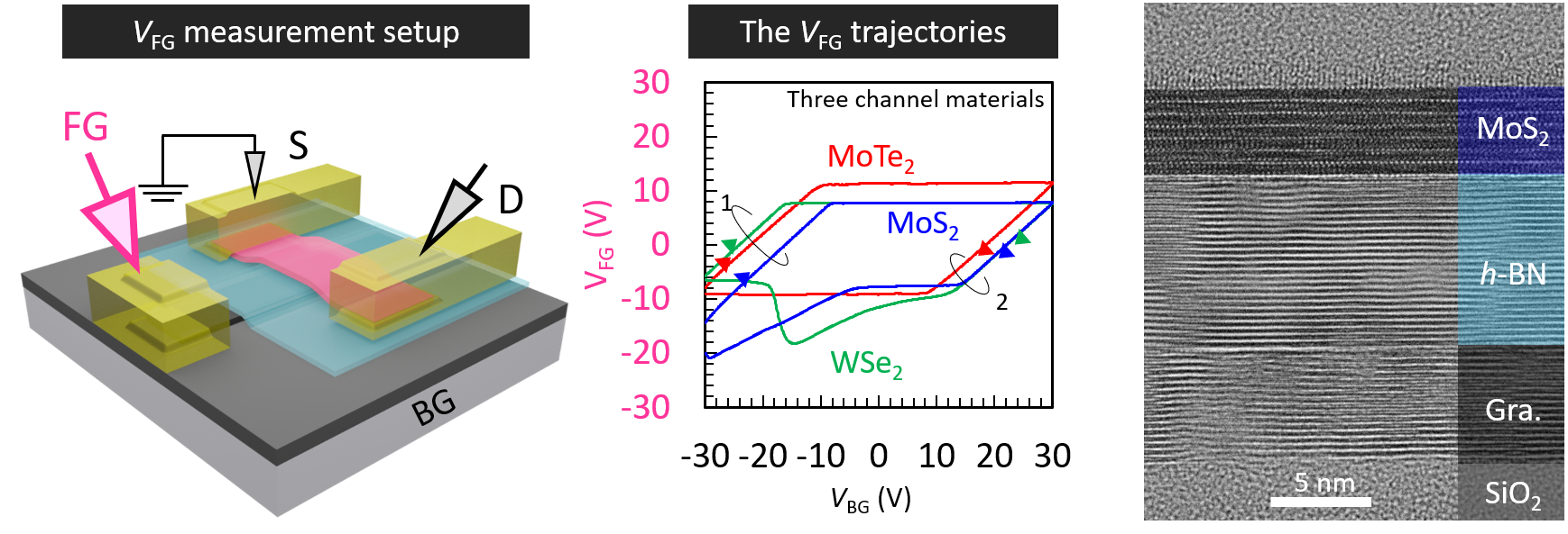
##(Left)Floating gate voltage measurement. (Middle) Trajectory of floating gate voltage during the round sweep of gate bias. By analyzing in detaild, the current limitting place for FN tunneling in the sevice can be detected. (right) Cross-sectional TEM. (Sasaki, 2021) SSDM Young Researcher’s award 2021.9
Ref.
T. Sasaki, K. Ueno, T. Taniguchi, K. Watanabe, T. Nishimura, K. Nagashio, “Material and Device Structure Designs for 2D Memory Devices Based on the Floating Gate Voltage Trajectory”, ACS nano, 2021, 15, 6658.
T. Sasaki, K. Ueno, T. Taniguchi, K. Watanabe, T. Nishimura, and K. Nagashio, “Understanding the Memory Window Overestimation of 2D Materials Based Floating Gate Type Memory Devices by Measuring Floating Gate Voltage”, small, 2020, 16, 2004907.
Taro Sasaki, Keiji Ueno, Takashi Taniguchi,Kenji Watanabe, Tomonori Nishimura, Kosuke Nagashio, “Ultrafast Operation of 2D Heterostructured Nonvolatile Memory Devices Provided by the Strong Short-Time Dielectric Breakdown Strength of h-BN”, ACS Appl. Mater. Interfaces., 2022, 14, 22, 25659–25669.
5. Layer-by-layer dielectric breakdown of h-BN & Powder device application
h-BN is considered to be ideal substrate & dielectric for layered channel materials. However, the study on dielectric breakdown is quite limitted.[collaborated with Dr. Taniguchi & Dr. Watanabe @NIMS]
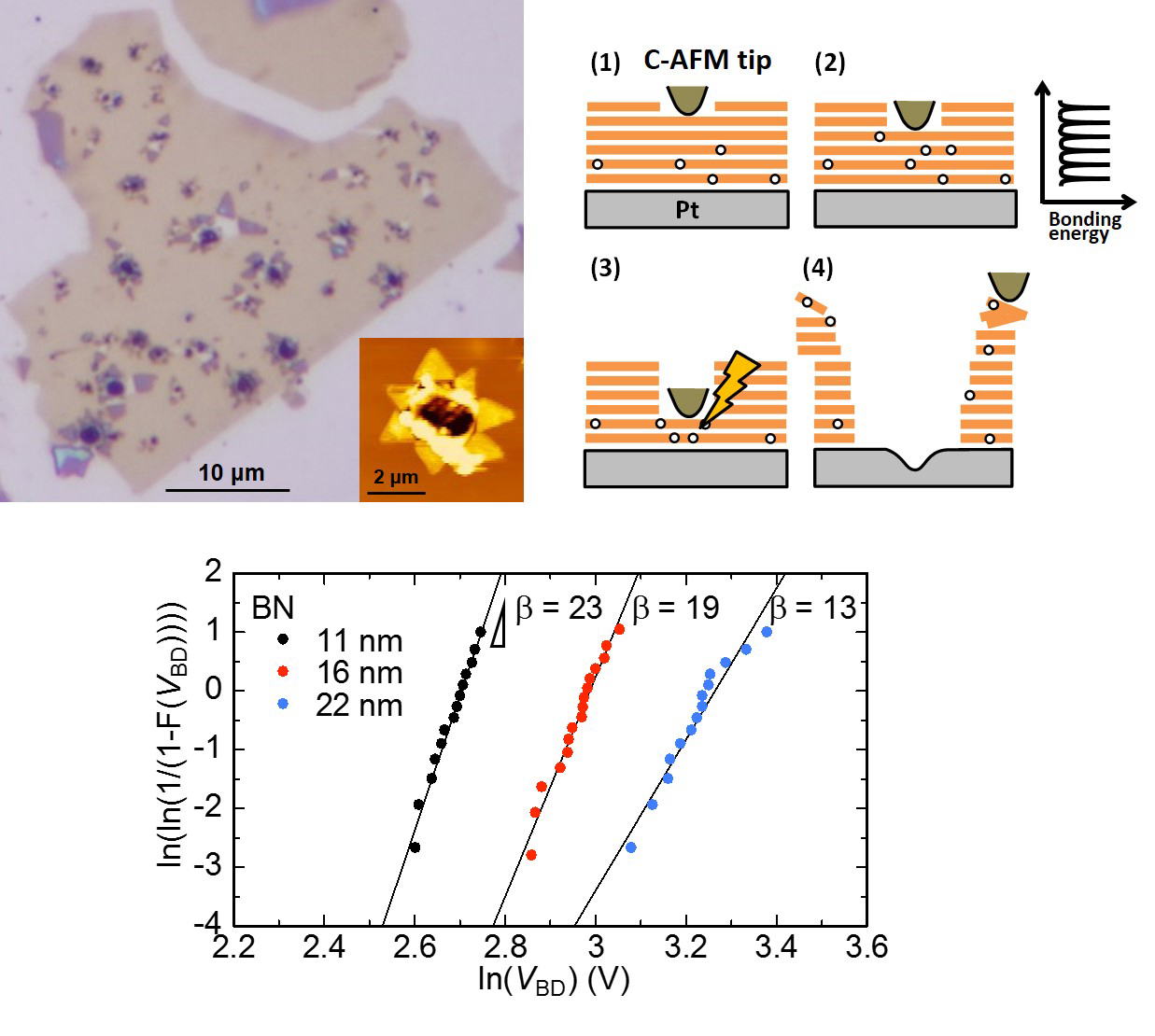
##(Left) Optical micrograph of electricaly broken h-BN. Prefered fracture direction could be armchair and/or zigzag direction. ##(right) h-BN undergoes layer-by-layer breakdown due to the bonding periodicity (covalent and van der Waals). ##(bottom) Weibull plot of breakdown voltage for different thickness of h-BN, suggesting that the unisotropic formation of defects is key to the layer-by-layer breakdown. (Hattori, 2014) JSAP young researcher award
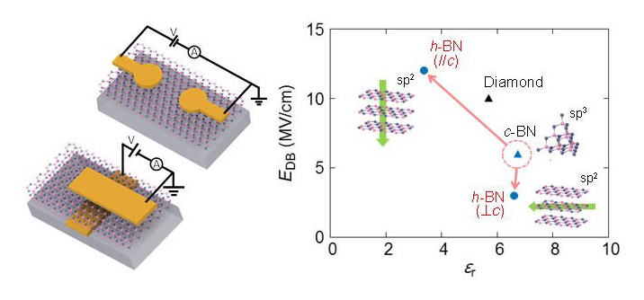
##(Left) Schematic of h-BN devices with two different breakdown direction. (Right) h-BN exhibits quite strong unisotropy of dielectric breakdonw field. The breakdown field of the vertical direction is stronger than that of diamond.
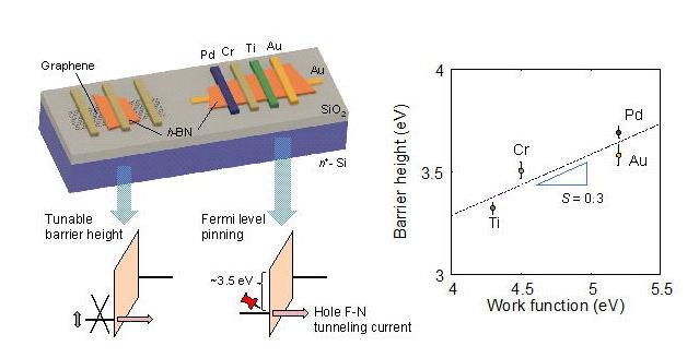
##(Left) Schematic of h-BN device with different metal electrodes (different work function). (Right) Estimated Barrier height as a function of work function. S factor is 0.3, suggesting the storng Fermi level pinning for h-BN.
Ref.
Y. Hattori, T. Taniguchi, K. Watanabe, K. Nagashioi, "Layer-by-layer dielectric breakdown of hexagonal Boron Nitride", ACS nano, 2015, 9, 916.
Y. Hattori, T. Taniguchi, K. Watanabe, and K. Nagashio, "Anisotropic breakdown strength of single crystal hexagonal Boron Nitride", ACS appl. mater. interfaces, 2016, 8, 27877.
Y. Hattori, T. Taniguchi, K. Watanabe, and K. Nagashio, "Comparison of device structures for the dielectric breakdown measurement of hexagonal boron nitride", Appl. Phys. Lett., 2016, 109, 253111.
K. Nagashio, Y. Hattori, N. Takahashi, T. Taniguchi, K. Watanabe, J. Bao, W. Norimatsu, and M. Kusunoki, Electrical Integrity and Anisotropy in Dielectric Breakdown of Layered h-BN Insulator, ECS Transactions, 2017, 79, 91-97.
Y. Hattori, T. Taniguchi, K. Watanabe, and K. Nagashio, “Impact ionization and transport properties of hexagonal boron nitride in constant-voltage measurement”, Phys. Rev. B, 2018, 97, 045425.
Y. Hattori, T. Taniguchi, K. Watanabe, and K. Nagashio, "Determination of Carrier Polarity in Fowler-Nordheim Tunneling and Evidence of Fermi Level Pinning at the Hexagonal Boron Nitride/Metal Interface", ACS appl. mater. interfaces, 2018, 10, 11732.
Supawan Ngamprapawat, Jimpei Kawase, Tomonori Nishimura, Kenji Watanabe, Takashi Taniguchi, and Kosuke Nagashio, ” From h-BN to graphene: characterizations of hybrid carbon-doped h-BN for applications in electronic and optoelectronic devices”, Adv. Electronic Mater., 2023, 2300083.
Supawan Ngamprapawat, Tomonori Nishimura, Kenji Watanabe,Takashi Taniguchi, Kosuke Nagashio, “Current Injection into Single-crystalline Carbon-doped h-BN toward Electronic and Optoelectronic Applications”, ACS Appl. Mater. Interfaces., 2022, 14, 22, 25731–25740.
Graphene research toward electronic devices
1. From graphite to graphene
We fabricate graphene FET by mechanical exforiation of Kish graphite.
## Optical micrograph (Left) and schematic diagram (right) of graphene FET by EB lithography.
To understand the whole picture from graphite to graphene is important!
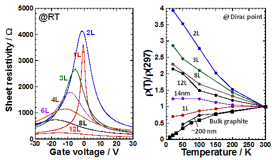
##(Left) Layer number dependence of sheet resistivity. Sheet resistivity monotonically increases with a decrease in the layer number. “L” indicates the number of layer.
##The continuous change of the normalized sheet resistivity from graphite to bilayer is governed by one unique property, i.e., the band overlap energy. JSAP paper awards
Ref.
K. Nagashio, T. Nishimura, K. Kita, and A. Toriumi, Appl. Phys. Express, 2009, 2, 025003.
K. Nagashio, T. Nishimura, K. Kita, and A. Toriumi, Jpn. J. Appl. Phys. 2010, 49, 051304.
2. Graphene/SiO2 interaction
Different SiO2 surface structures interact with graphene differently.
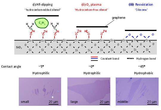
##Hydrophobic & hydrophilic surfaces can be obtained by the surface treatments of SiO2. The size of graphene obtained by mechanical exfoliation is different. (Yamashita, 2011)
Ref.
K. Nagashio, T. Yamashita, T. Nishimura, K. Kita, and A. Toriumi, J. Appl. Phys. 2011, 110, 024513.
K. Nagashio, T. Yamashita, T. Nishimura, K. Kita, and A. Toriumi, "Impact of graphene/SiO2 interaction on FET mobility and Raman spectra in mechanically exforiated graphene films", IEEE International Electron device meeting (IEDM) Tech. Dig. 2010, 564.
3. Understanding & control of graphene/metal contact
Contact resistivity is expected to be one of main limiting factors.
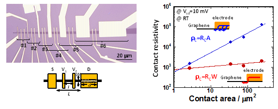
##(Left) Optical micrograph of the four-layer graphene device with six sets of four-probe configurations (#1~#6). The contact metal is Ni. (Right) Two types of contact resistivity (RCA & RCW) extracted by a four-probe measurement from the devices [left figure]. This result indicates that the current injection take place at the edge (red).
Density of states of graphene in contact with metal are different for chemisorption and physisorption!
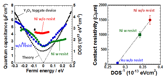
##(Left) Extracted DOS of graphene in contact with metal by quantum capacitance measurement. For Ni/graphene, DOS of graphene increased due to chemisorption, while DOS of graphene in contact with Au did not change due to physisorption. (Right) Correlation between DOS and contact resistivity. Contact resistivity is controlled by DOS of graphene. (Ifuku, 2013, JSAP young researcher award).
Ref.
K. Nagashio, T. Nishimura, K. Kita, and A. Toriumi, "Metal/graphene contact as a performance killer of ultra-high mobility graphene – analysis of intrinsic mobility and contact resistance -", IEEE International Electron device meeting (IEDM) Tech. Dig. 2009, 565.
K. Nagashio, T. Moriyama, R. Ifuku, T. Nishimura, and A. Toriumi, "Is graphene contacting with metal still graphene?", IEEE International Electron device meeting (IEDM) Tech. Dig. 2011, 27.
K. Nagashio, R. Ifuku, T. Moriyama, T. Nishimura, and A. Toriumi, "Intrinsic graphene/metal contact", IEEE International Electron device meeting (IEDM) Tech. Dig. 2012, 68.
K. Nagashio, T. Nishimura, K. Kita, and A. Toriumi, Appl. Phys. Lett. 2010, 97, 143514.
T. Moriyama, K. Nagashio, T. Nishimura, and A. Toriumi, J. Appl. Phys. 2013, 114, 024503.
R. Ifuku, K. Nagashio, T. Nishimura, and A. Toriumi, Appl. Phys. Lett. 2013, 103, 033514.
[Invited review] K. Nagashio, and A. Toriumi, Jpn. J. Appl. Phys. 2011, 50, 070108.
[Book] K. Nagashio, A. Toriumi, "Graphene/metal contact" in Frontiers of graphene and carbon nanotubes, Springer, 2015, pp.53-78.
4. Improvement of high-k top gate insulator and CQ measurement
Based on the thermodynamic consideration, Y2O3 is selected as top-gate insulator for graphene FET. Low field leakage current density is drastically reduced by high-pressure O2 post-deposition annealing.
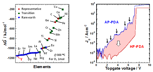
##(Left) Standard Gibbs free energy change for oxidation reaction. Y metal has lowest value. Y2O3 is selected as top-gate insulator. (Right) Leakage current density for Y2O3 top-gate graphene FET (Y2O3: ~5nm). High-pressure O2 post deposition annealing (HP-PDA @100atm) reduce Jg, compared with atmospheric pressure-PDA (AP-PDA@1atm).
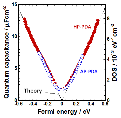
##Quantum capacitance as a function of EF from C-V measurement. Large EF modulation in graphene (EF=~0.52 eV) is achieved by drastic improvement of topgate insulator quality. (Kanayama, 2013)
Ref.
K. Kanayama, K. Nagashio, T. Nishimura, and A. Toriumi, Appl. Phys. Lett. 2014, 104, 083519.
K. Nagashio, T. Nishimura, and A. Toriumi, Appl. Phys. Lett. 2013, 102, 173507.
5. CVD growth of graphene
Large area monolayer graphene is grown on Cu(111)/mica.
##(Left) Raman data for CVD graphene transfered on SiO2/Si substrte. D band intensity is reduced considerably. (Right) Mobility estimated from 4-probe measurement. Max. mobility is ~4,500 cm2/Vs.
(Qi, 2013)
Ref.
J. L. Qi, K. Nagashio, T. Nishimura, and A. Toriumi, Nanotechnology, 20014, 25, 185602.
6. high-k oxide deposition on layered materials by ALD
It is difficult to deposit high-k oxide by ALD on layered materials, such as graphehe due to chemical inertness of surfaces. The physical adsorption of precursor is possible for h-BN since it is porlarized. We are studying the direct deposition of ALD Y2O3 on layered materials.
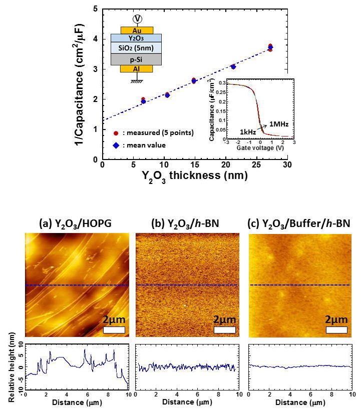
##(Top)1/C plot for Y2O3/SiO2/Si capacitor as a fuction of Y2O3 thickness. The inset shows the CV result. The slope indicates the dielectric constant for ALD-Y2O3. ##(Bottom)ALD-Y2O3 on (a) HOPG, (b) h-BN, and (c) buffer layer/h-BN. (Takahashi, 2014)
Ref.
N. Takahashi, T. Taniguchi, K. Watanabe, K. Nagashioi, "Atomic layer deposition of Y2O3 on h-BN for a gate stack in graphene FETs", Nanotechnology, 2015, 26, 175708.
N. Takahashi, and K. Nagashio, "Buffer Layer Engineering on Graphene via Various Oxidation Methods for Atomic Layer Deposition", Appl. Phys. Express, 2016, 9, 125101.
7. Transport in bilayer graphene & Gap state analysis
A. High-k Y2O3/BLG FET
Energy gap can be formed by external electrical field to bilayer graphene. It is well known that Ion/off is quite small due to gap states. Here, we applied high pressure O2 annealing to Y2O3 to improve the top gate high-k quality. High Ion/off was obtained and gap state density was analyzied for the first time.
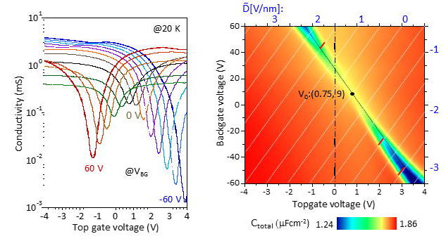
##(Left) Conductivity as a function of top gate voltage. Ion/off of 3*103 was obtained @ VBG=-60V. (Right) 3D map of source-topgate total capacitance . The decrease in CTotal is observed by the decrease in DOS due to gap opening.
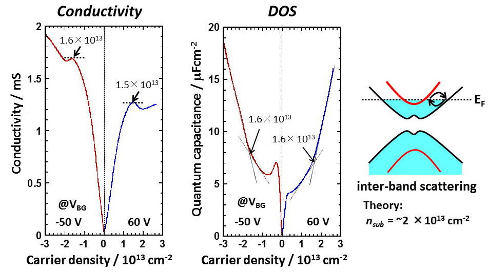
##Using high-quality Y2O3 top gate, Fermi level can be modulated upto upper subband in bilayer graphene. The conductivity reduciton is observed due to subband scattering, while the change of slope of DOS is observed due to the transition from bottom to upper subband. These change was observed at the same carrier density.
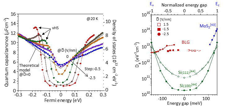
##(Left) Quantum capacitance measurment of bilayer graphene. Band gap opening is clearly seen with increasing the displacement field D (V/nm). (Right) Gap state density as a funciton of energy gap, which is measured by conductance method. The origin for gap states could be trap sites in top gate oxide and/or AB stack breaking. (Kanayama, 2014).
B. All 2D hetero BLG FET
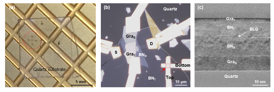
##(Left) BLG FET devices were prepared on quartz substrate to remove the parasitic capacitance. (Middle) All 2D hetero BLG FET on quartz substrate.. (Right) Xsectional TEM image of all 2D hetero. (Uwanno, 2018).
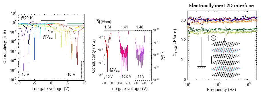
##(Left) Large Ion/off ratio was obtained in all 2D hetero FET. The conductivity reaches the measurment limitation. (Right) Capacitance as a function of frequency. No frequency dispersion was seen in conductance measurment. (Uwanno, 2018).
Ref.
[Review] K. Nagashio, “Graphene field-effect transistor application -Electric band structure of graphene in transistor structure extracted from quantum capacitance-“, J. Mater. Res. 2017, 32, 64.
K. Kanayama, and K. Nagashio, “Gap state analysis in electric-field-induced band gap for bilayer graphene”, Sic. Rep. 2015,5, 15789.
K. Nagashio, K. Kanayama, T. Nishimura, and A. Toriumi, “Quantum capacitance measurement of bilayer graphene”, ECS Trans. 2014, 61(3), 75.
K. Nagashio, K. Kanayama, T. Nishimura, and A. Toriumi, “Carrier response in band gap and multiband transport in bilayer graphene under the ultra-high displancement”, IEEE International Electron device meeting (IEDM) Tech. Dig. 2013, 503.
T. Uwanno, T. Taniguchi, K. Watanabe, & K. Nagashio, “Electrically inert h-BN/bilayer graphene interface in all-2D-heterostructure FETs”, ACS appl. mater. interfaces, 2018, 10, 28780.
8. Fully dry transfer technique for 2D heterostructures
Based on the experimental results of gap state analysis, FET device research also requires h-BN substrates. Generally, for the 2D heterostructure fabrication, PMMA is dissolved after the position adjustment. But the PMMA residue degrades the transport properties. Here, we establish the fully PMMA dry transfer using the difference in thermal expansion coefficient for polymers and inorganic materials.
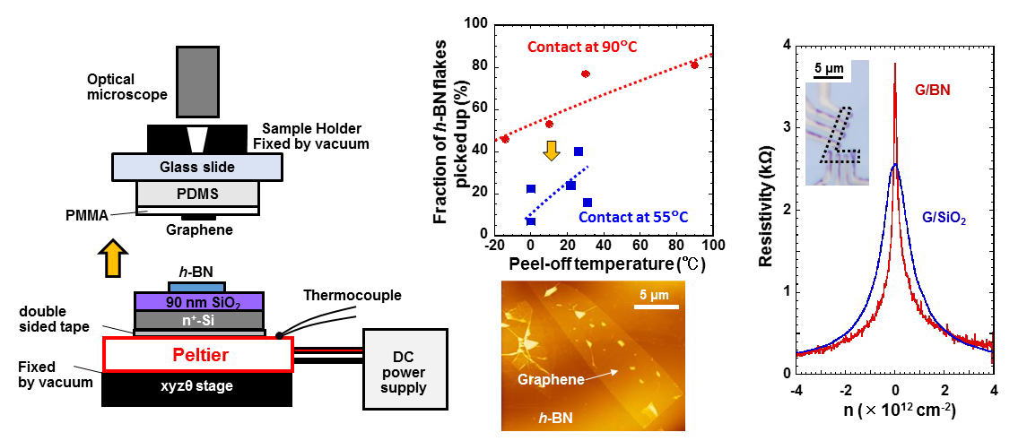
##(Left) Transfer apparatus with temperature controller. (Middle) The best condition for transfer is 55C for the contact and 15C for peeling off. The bubbles due to hydrocarbons at the interface of graphene and h-BN are clearly seen due to no residue of PMMA. (Right) Transport properties of graphene on SiO2 and h-BN. (Uwanno, 2015)
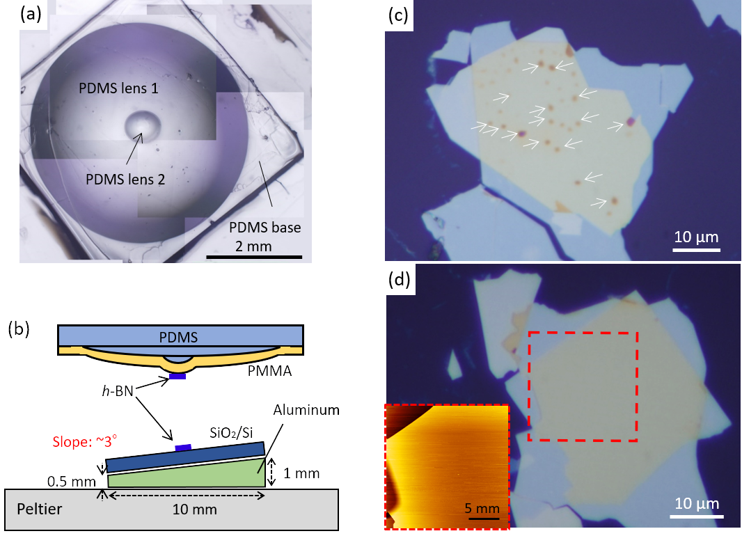
##(a) Pinpoint pick up and transfer can be possible using PDMS with the lens shape. (b) Bubble free transfer is achieved by the slope, because the unidirectional sweep of the transfer interface is possible. (c) For the transfer without slope, many bubbles are incorporated. (d) For the transfer with slope, bubble free transfer is possible. (Toyoda, 2019)
Ref.
T. Uwanno, Y. Hattori, T Taniguchi, K Watanabe and K Nagashio, "Fully dry PMMA transfer of graphene on h-BN using a heating/cooling system", 2D mater. 2015, 2, 041002. Highlight of 2015
S. Toyoda, T. Uwanno, T. Taniguchi, K. Watanabe, and K. Nagashio, "Pinpoint pick-up and bubble-free assembly of 2D materials using PDMS/PMMA polymers with lens shapes", Appl. Phys. Express, 2019, 12, 055008.
9. Transport properties of high-k nanosheet
We have studied high-k nanosheet on 2D channel and electrical properties of high-k nanosheet.[collaborated with Dr. Osada @Nagoya Univ.]
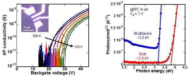
##(Left) TiOx nanosheet has been transformed into anatase thorugh the solid state transformation by annealing. Anatase shows n-type FET characteristics. (Right) TiOx nanosheet includes almost no O vacancies due to excess Ti. From the photocurrent data, the O vacancy contents are quite small because typical O vacancy related peak at ~2 eV has not been observed. (2017 Sekizaki)
Ref.
S. Sekizaki, M. Osada, and K. Nagashio, “Molecularly-thin Anatase field-effect transistors fabricated through the solid state transformation of titania nanosheets”, Nanoscale, 2017, 9, 6471–6477.